Lith Corporation, founded in 1998 by a group of material science doctor from Tsinghua University, has now become the leading manufacturer of battery lab&production equipment. Lith Corporation have production factories in shenzhen and xiamen of China.This allows for the possibility of providing high quality and low-cost precision machines for lab&production equipment,including: roller press, film coater,mixer, high-temperature furnace, glove box,and complete set of equipment for research of rechargeable battery materials. Simple to operate, low cost and commitment to our customers is our priority.
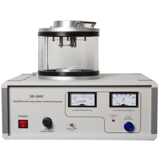
PVD Sputtering Coating: Overview, Features, Process, Applications, Advantages, and Conclusion
PVD Sputtering Coating is a highly advanced thin-film deposition technology widely used in both industrial manufacturing and research applications. As a type of Physical Vapor Deposition (PVD), it relies on the sputtering process to transfer atoms from a solid target onto a substrate, forming dense, uniform, and adherent films. This technique has become critical in industries requiring precise surface modification, including microelectronics, optics, surface engineering, energy devices, and analytical equipment preparation.
Overview
A PVD Sputtering Coating system operates by generating a plasma within a vacuum chamber, typically using an inert gas such as argon. Ions from the plasma bombard the target material, ejecting atoms that travel across the chamber and deposit onto the substrate surface. Unlike conventional coating methods, PVD sputtering allows for deposition of a wide range of materials, including metals, alloys, and even some insulating compounds, with excellent control over thickness, composition, and microstructure. Modern systems often incorporate magnetron sputtering sources to enhance deposition efficiency and film uniformity.
Key Features of PVD Sputtering Coating Systems
The efficiency and versatility of PVD Sputtering Coating systems stem from several key design features:
High-Vacuum Chamber: Minimizes contamination and ensures high-purity film formation.
Magnetron or Planar Targets: Increase plasma density near the target for high sputtering rates while reducing substrate heating.
Multiple Power Modes: DC, RF, and pulsed-DC allow deposition of both conductive and insulating materials.
Automated Substrate Manipulation: Rotation, tilting, or biasing ensures uniform film thickness over complex surfaces.
Integrated Process Control: Real-time monitoring of deposition rate, film thickness, gas flow, and plasma parameters enhances reproducibility.
These features collectively ensure precise, reliable, and high-quality coatings suitable for a variety of applications.
PVD Sputtering Coating Process
The sputtering process begins with evacuating the chamber to a high vacuum, by the introduction of a working gas such as argon. A high-voltage potential applied to the target generates plasma, which produces positively charged ions. These ions accelerate toward the target, dislodging atoms from the target material via momentum transfer. The sputtered atoms then condense onto the substrate, forming a thin, adherent coating.
Several variations of the PVD sputtering process are employed depending on material and application requirements:
DC Sputtering: Used for conductive metals, providing high deposition rates.
RF Sputtering: Enables deposition of insulating materials and ceramics.
Reactive Sputtering: Involves reactive gases like oxygen or nitrogen to form compounds such as oxides, nitrides, or carbides.
Co-Sputtering: Allows simultaneous deposition from multiple targets to produce alloys or composite films.
These variations provide flexibility in tailoring coating properties to meet specific industrial or research demands.
Nano PVD System
Applications
PVD Sputtering Coating is applied across multiple sectors due to its versatility and high-quality output:
Microelectronics & Semiconductors: Deposition of conductive, dielectric, and barrier layers on wafers, circuits, and MEMS devices.
Optics & Photonics: Anti-reflective coatings, mirrors, optical filters, and protective layers for lenses and displays.
Energy & Environmental Devices: Fabrication of thin-film solar cells, battery electrodes, and transparent conductive oxides (TCOs).
Surface Engineering: Hard coatings, wear-resistant layers, corrosion protection, and decorative finishes on metals, plastics, and ceramics.
Analytical Instruments: Coating of SEM or AFM samples to improve conductivity and imaging resolution.
Advantages
The advantages of PVD Sputtering Coating include:
Uniform and High-Quality Films: Produces smooth, dense coatings with strong adhesion.
Material Versatility: Compatible with metals, alloys, semiconductors, and some insulators.
Low Substrate Temperature: Suitable for temperature-sensitive materials such as polymers or electronics.
Excellent Reproducibility: Automated control systems ensure consistent film thickness and properties.
Minimal Contamination: High-vacuum operation reduces oxidation and impurity incorporation.
Conclusion
In conclusion, PVD Sputtering Coating represents a versatile, reliable, and high-performance technology for thin-film deposition. Its ability to produce dense, uniform, and adherent coatings across a broad range of materials makes it indispensable in electronics, optics, energy devices, surface engineering, and research laboratories. By offering precise control over film thickness, composition, and microstructure while minimizing substrate heating, PVD Sputtering Coating continues to play a critical role in advancing modern material science and industrial surface engineering.


 +86 13174506016
 Louis@lithmachine.com
 +86 18559646958
 18659217588
 English ▼


